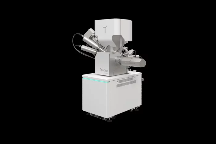
TESCAN Plasma FIB-SEM, AMBER X2
Automated TEM Lamella Preparation
FIB-SEM Analysis, Fast and Precise
Novel 3D Multimodal Insights
Advanced Contrast Methods
TESCAN Plasma FIB-SEM, AMBER X2
Advanced Semiconductor Delayering
Electron Beam Resolution :
1.4nm at 1keV, 0.9nm at 15keV
Ion Beam Resolution :
10nm at 30keV, 200nm at 1keV
Products & Services
TESCAN AMBER 2
Tescan Group a.s.
Tescan AMBER integrates BrightBeam™ field-free SEM optics with the Orage™ Ga⁺ FIB and fully automated lamella workflows. Designed for versatility, it supports inverted and planar sample prep, nanoprototyping, and gentle final polishing across a wide range of material types.
TESCAN SOLARIS 2
Tescan Group a.s.
TESCAN SOLARIS is a fully automated sample prep platform optimized for advanced devices with sub-10 nm features. It integrates the Triglav™ SEM, AutoTEM Pro™ software, and OptiLift™ nanomanipulator to enable hands-free, repeatable lamella prep in planar, inverted, or top-down geometries.
TESCAN Plasma FIB-SEM, SOLARIS X2
Tescan Group a.s.
TESCAN SOLARIS X 2 extends FIB physical failure analysis capabilities to large-area applications, making deep cross-sectioning of advanced packaging devices, displays, MEMS, and optoelectronic devices more efficient.
Featuring the new generation Mistral™ Xe Plasma FIB column, SOLARIS X 2 offers increased maximum ion beam current and a sharper ion beam profile across the full range, with significantly reduced beam tails. This allows operators to use higher milling and polishing currents, achieving superior surface quality comparable to conventional Plasma FIB, but with greater speed and precision.
Featuring the new generation Mistral™ Xe Plasma FIB column, SOLARIS X 2 offers increased maximum ion beam current and a sharper ion beam profile across the full range, with significantly reduced beam tails. This allows operators to use higher milling and polishing currents, achieving superior surface quality comparable to conventional Plasma FIB, but with greater speed and precision.
TESCAN TENSOR
Tescan Group a.s.
Explore nanoscale structure with clarity, speed, and confidence.
Tescan’s STEM solutions are purpose-built for advanced materials research, semiconductor analysis, and detailed nanoscale characterization. With integrated 4D-STEM, precession-assisted diffraction, and synchronized EDS workflows, our instruments deliver actionable insight with unmatched usability—whether you're mapping strain, analyzing phases, or accelerating failure analysis and R&D.
Tescan’s STEM solutions are purpose-built for advanced materials research, semiconductor analysis, and detailed nanoscale characterization. With integrated 4D-STEM, precession-assisted diffraction, and synchronized EDS workflows, our instruments deliver actionable insight with unmatched usability—whether you're mapping strain, analyzing phases, or accelerating failure analysis and R&D.
TESCAN UniTOM HR
Tescan Group a.s.
Investigate the smallest of features with spatial resolution down to 600 nm – A state-of-the-art nano-focus x-ray source, precision stages, and high-quality detectors work together to deliver sub-micron resolution imaging.
Perform true 4D imaging with Dynamic CT – High temporal resolution, continuous and uninterrupted scanning, and specialized 4D software tools bring synchrotron-like capabilities to the lab.
Implement 3D in situ experiments – continuous sample rotation and scanning enable uninterrupted in situ experiments. Dedicated “no-cable-wrap” interfaces simplify experiment set-up.
Accommodate a broad range of samples – UniTOM HR’s high power source (50W), multiple detector options (up to 3) and heavy load stage (45 kg) accommodates samples up to 500 mm diameter X 700 mm high.
Maximize system utilization and throughput – A fast frame rate detector and a high flux x-ray source combine for high temporal resolution tomography giving you the ability to scan more samples and accommodate more users.
People
Description
An optimized Plasma FIB-SEM platform with proprietary gas chemistries for high-quality delayering of the most current semiconductor devices