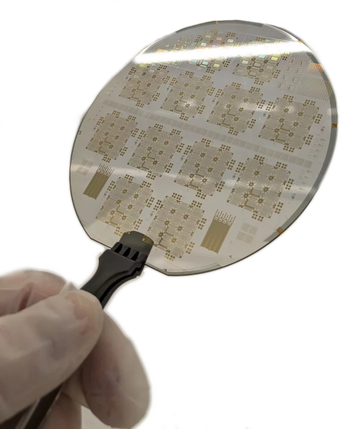
Next-gen GaN fabrication processes
>3x higher RF power density than existing GaN solutions
Ultra-high linearity and power-added efficiency
Best-in-industry turnaround times
License-free export to 32 countries
Next-gen GaN fabrication processes
• 300 nm RF GaN process for microwave applications to 30 GHz
• Scaled RF GaN process for mm-wave applications to 100 GHz
• Custom GaN processes for digital, power, and high-temp applications
People
Description
Our firm offers end-to-end GaN production capabilities, including fabrication, packaging, test, and failure analysis to meet custom requirements. To enable customer designs, a process design kit (PDK) is available with a design manual, sample layouts, and a non-linear device model. Options available include fabrication of customer-designed wafers (“PDK foundry service”) or custom design by TransEON and fabrication according to customer specs (“NRE foundry service”). For either option, volume levels available include pilot/engineering runs, multi-project wafers (MPWs), or full production runs.